
Copper Trace Design – PCB DFM Part 7
7.1 Trace Width, Spacing and Routing Requirements [65] The width and spacing of copper traces

Seeed Studio / CircuitMaker June 2017 Design Contest
CircuitMaker and Seeed Studio are collaboratively hosting a design contest based on Seeed’s Wio LTE

A Beginner’s Guide to DIYing with the ReSpeaker
Probably you might get a ReSpeaker from Kickstarter or Bazaar. It is a hack-able open

Solder Mask Design – PCB DFM Part 6
6.1 Solder Mask Design for Copper Traces [50] Generally, solder mask will cover copper traces,

How to Design a Circuit Board
It is exciting to learn how to design your circuit board, especially as newbies. We
Hole Design – PCB DFM Part 5
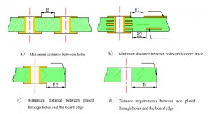
5.1 Vias 5.1.1 Hole Spacing Figure 31: Spacing requirements for holes and vias [44] The

Introducing the new Renesas S5D9 IoT Fast Prototyping Kit
Today, we are very pleased to announce the new Renesas S5D9 IoT Fast Prototyping Kit! In
Component Layout Considerations – PCB DFM Part 4
4.1 General Component Layout Requirements Through-hole components with polarity or direction requirements should maintain a

Good News: FREE PCB DFM manual available in Seeed Fusion
Dear all, Seeed is a hardware innovation platform for makers to grow inspirations into differentiating