Whether UAV or Amazon Alexa,all can made by BBG or BBGW
Probably you had heard or bought SeeedStudio BeagleBone Green & BeagleBone Green Wireless. Due to excellent specification, BBG &BBGW

Micro:bit Small-board Computer Launches in U.S. & Canada
We are so happy to share with you the exciting news! Micro:bit launches in U.S. and
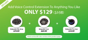
Time-limited bundle sales: ReSpeaker core + ReSpeaker Mic Array + Pro Case for only $128
Great news! You can now buy the ReSpeaker core, Mic Array and ReSpeaker Pro Case for
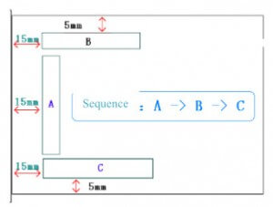
Silkscreen Design – PCB DFM Part 8
8.1 Silkscreen Design Considerations [77] General Requirements The width of the silkscreen line should be

Fusion Advanced PCB service launched in Seeed Fusion
We are proud to introduce Fusion’s new Advanced PCB service for designs of up to
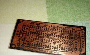
How to Make PCB Circuit Board at Home
Do you want to make a Printed Circuit Board by yourself? Maybe you are a student,
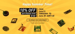
Enjoy 10% OFF your purchase of $100 [COUPON CODE: SEEEDSUMMER]
Let’s celebrate summer time with a screaming deal on Seeedstudio Bazaar! You can enjoy 10% Discount
We will no longer use Singapore Post delivery service for Canada
Fusion has made the decision not to use Singapore Post for delivery to Canada. Please
FREE PCB DFM Manual V1.1 Available In Seeed Fusion
Dear Fusion Users, Thank you for all your feedback. We are pleased to announce that