
Solder Mask Design – PCB DFM Part 6
6.1 Solder Mask Design for Copper Traces [50] Generally, solder mask will cover copper traces,

How to Design a Circuit Board
It is exciting to learn how to design your circuit board, especially as newbies. We
Hole Design – PCB DFM Part 5
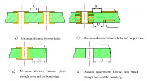
5.1 Vias 5.1.1 Hole Spacing Figure 31: Spacing requirements for holes and vias [44] The

Introducing the new Renesas S5D9 IoT Fast Prototyping Kit
Today, we are very pleased to announce the new Renesas S5D9 IoT Fast Prototyping Kit! In
Component Layout Considerations – PCB DFM Part 4
4.1 General Component Layout Requirements Through-hole components with polarity or direction requirements should maintain a

Good News: FREE PCB DFM manual available in Seeed Fusion
Dear all, Seeed is a hardware innovation platform for makers to grow inspirations into differentiating
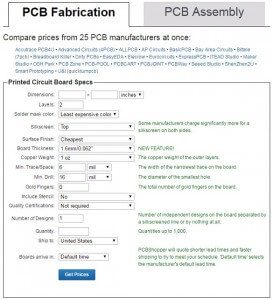
PCB Cost Calculator for Estimating the Cost of PCB Manufacturing and Assembly
Price, quality, delivery time and service are the most common criteria engineers concern when choosing
Panelization and Bridge Design – PCB DFM Part 3
In this post we will learn the part 3: Panelization and Bridge Design. If you have
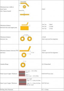
Seeed Fusion PCB Specification – PCB DFM Part 2
Seeed Fusion PCB Specification 2.1 PCB Gerber File The Gerber format is an open 2D