I2C Communication Protocol and How It Works
Maybe you have heard about I2C or you have already used I2C before, but have you ever understood what I2C is? How does I2C work? This blog will show you this I2C knowledge.
What Is I2C
I²C (Inter-Integrated Circuit) is a serial communication bus that uses a multi-master-slave architecture. It was designed by Philips in the early 1980s (now NXP Semiconductors). I2C is convenient for motherboards, embedded systems, or Communication between cell phones and peripheral components. Due to its simplicity, I2C is widely used for communication between microcontrollers and sensor arrays, displays, IoT devices, EEPROMs, etc. I2C consists of two lines, SCL and SDA. These two data lines need to be connected to pull-up resistors. When the bus is idle, SCL and SDA are at a high level. The I2C bus works according to a certain protocol. Next, let’s take a look at the I2C protocol. I2C supports multiple slaves, that is, multiple I2C slave devices can be attached to one I2C controller. These different I2C slave devices have different device addresses so that the I2C master controller can access the specified device address through the device address of the I2C device. I2C device, one I2C bus connects multiple I2C devices as shown in the figure:
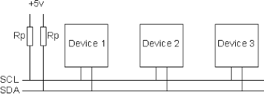
SDA and SCL links must be connected to a pull-up resistor, usually 4.7K. The rest of the I2C slaves are hooked up to the SDA and SCL lines so that multiple I2C devices can be accessed via the SDA and SCL lines.
Maybe you are still confused about I2C, here are some features of I2C
Features of I2C:
1. Only one data line SDA and one clock line SCL are required, SDA (serial data line) and SCL (serial clock line) are both bidirectional I/O lines
SCL (Serial Clock): Serial clock line, which transmits CLK signals, generally provided by the master device to the slave device
SDA (Serial Data): serial data line, transmit communication data
2. Realize a real multi-master bus, any device can be used as both a master and a slave, but there can only be one master at the same time
3. It can be detected by external connection, which is convenient for system fault diagnosis and debugging
4. ICs connected to the same bus are only limited by the maximum capacitance of the bus. The serial 8-bit bidirectional data transfer bit rate can reach 100Kbit/s in standard mode, 400Kbit/s in fast mode, and up to 3.4Mbit/s in high-speed mode.
5. The current consumed on the bus is very small. Therefore, the number of devices expanded on the bus is mainly determined by the capacitive load, which is resistant to high noise interference. Adding a bus driver can expand the bus capacitance by 10 times, and the transmission distance can reach 15m; compatible with different voltage levels devices with a wide operating temperature range
6. The interface circuit is an open-drain output. It needs to be connected to the power supply VCC through a pull-up resistor. When the bus is idle, both lines are high. The external devices connected to the bus are CMOS devices. The output stage is also an open-drain circuit.
Data Transmission:
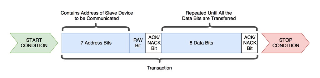
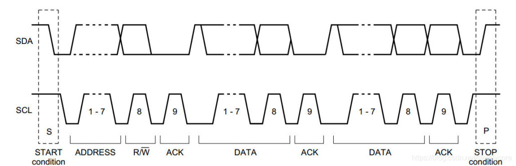
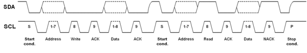
The master device and slave device follow the following protocol format for data transmission. Data transfer serial data of 0 and 1 between the master and slave devices over an SDA data line, The structure of a serial data sequence can be divided into:
- Start Bit
- Address Bits(7bit or 10bit)
- Read and Write Bit(1bit)
- Response Bit (1bit)
- Data bit + response bit (data bit 8bit; response bit 1bit; data + response can be repeatedly transmitted many times until encountering the stop bit)
- Stop Bit
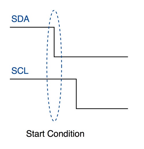
Start Bit
When the master device decides to start communication, it needs to send a start signal, and the following actions need to be performed
- First, switch the SDA from VOH to VOL
- Then change SCL from VOH to VOL
After the master device has signaled and started condition, all slaves will become active even in sleep mode and wait to receive an address bit.
Address Bit
Address bits support 7bit and 10bit, If the master needs to send/receive data to the slave, it must send the address first then the slave will correspond, and then match the address of the slave mounted on the bus.
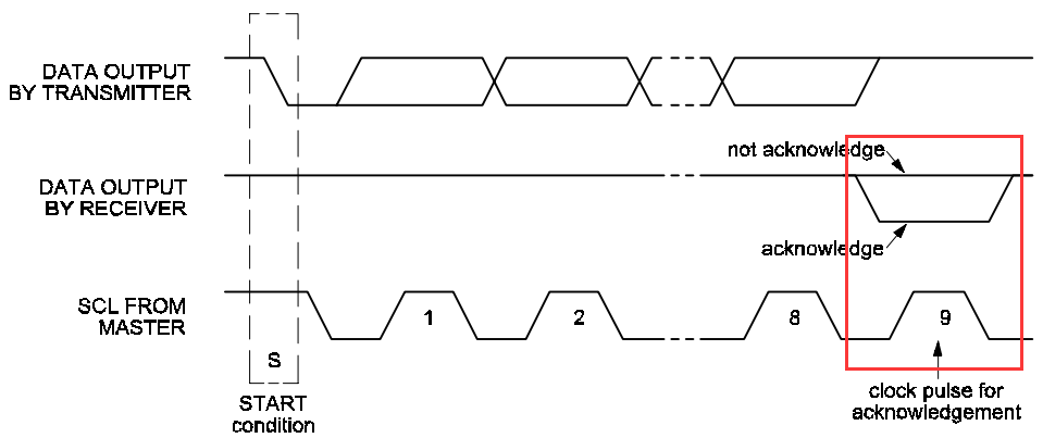
Response Bit
Response Bit has 2 types:
- ACK: Slave correctly receives data or address bit + read and write bits
- NACK: slave does not answer and works abnormally
Every time the master sends data and read and write bits, it will wait for the response signal ACK from the slave device.
- If the slave device sends the response bit signal ACK
- If there is no response signal NACK, SDA will output a VOH, which will cause the master device to reboot or stop
Data Bit
Every time the data is transmitted has a total of 8 bits, which the sender sets and it needs to transmit the data bits to the receiver.
The transmission is followed by an ACK/NACK bit, and if the receiver successfully receives the data, the slave sends an ACK. Otherwise, the slave sends a NACK.
Data can be sent multiple times until a stop bit is received.
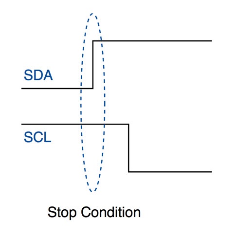
Stop Bit
When the master device decides to end the communication, it needs to send the end signal, and the following actions need to be performed.
- First switch the SDA from a VOL to VOH
- Then the SCL switches from VOH to VOL
Here’s the figure showing the completed I2C timing diagram:
Multi-Main Arbitration
In a multi-main communication system. There are multiple nodes on the bus, they all have their own addressing addresses, they can be accessed by other nodes as slave nodes, and they can all be used as master nodes to send control bytes and transfer data to other nodes. But if two or more nodes both send start signals to the bus and start transmitting data, a conflict occurs. To resolve this conflict, an arbitration decision is required, which is arbitration on the I2C bus.
The arbitration on the I2C bus is divided into two parts: the synchronization of the SCL line and the arbitration of the SDA line.
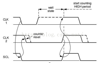
Synchronization of The SCL Line (Clock Synchronization)
SCL synchronization is due to the logic function of the bus line “AND” (open-drain output), that is, as long as one node sends a low level, the bus appears as a low level. The bus can only appear high when all nodes send high. It is precise because of the principle of the line “AND” logic function that when multiple nodes send clock signals at the same time, a unified clock signal is displayed on the bus. This is the synchronization principle of SCL
SDA Arbitration
Arbitration of the SDA line is also based on the principle that the bus has a line “AND” logic function. After the node sends 1-bit data, it compares whether the data presented on the bus is consistent with what it sent (similar to the readback mechanism of the CAN bus). Yes, continue sending; otherwise, exit the competition. Arbitration of the SDA line can ensure that the I2C bus system communicates normally and data is not lost when multiple master nodes attempt to control the bus at the same time. The bus system allows only one master node to continue to occupy the bus through arbitration.
Arbitration Process
DATA1 and DATA2 are respectively the data signals sent by the master node to the bus, SDA is the data signal presented on the bus, and SCL is the clock signal presented on the bus. When master nodes 1 and 2 send start signals at the same time, both master nodes send high-level signals. At this time, the signal on the bus is high, and both master nodes detect that the signal on the bus is the same as the signal sent by themselves, and continue to send data. In the second clock cycle, both master nodes send low-level signals, and the signals presented on the bus are low-level and continue to send data. In the 3rd clock cycle, master node 1 sends a high-level signal, while master node 2 sends a low-level signal. According to the logic function of the line “AND” of the bus, the signal on the bus is low level. At this time, master node 1 detects that the data on the bus is different from the data sent by itself, and disconnects the output stage of the data, and turns to The slave to receive the status. In this way, master node 2 wins the bus, and the data is not lost, that is, the data on the bus is the same as the data sent by master node 2, and master node 1 continues to receive data after turning into a slave node, and also does not lose the SDA line. data. Therefore data is not lost during the arbitration process.
Summary: SDA arbitration and SCL clock synchronization processing are not sequential, but are carried out at the same time.
I2C Deadlock
In actual use, I2C is prone to deadlock. There are two common situations in which deadlocks occur:
- One is that the master device resets abnormally when the slave device replies ACK
- The other is that the master device resets abnormally when the slave device replies with a data bit of 0
The same point in both cases is that SDA is in a state of being pulled low by the slave device when the master device is reset abnormally, while SCL is in a VOH (idle state) after the master device is reset. At this point, the slave device will wait for the master device to pull SCL low to take the ACK or data bit, and the master device will wait for the slave device to release the SDA line. The master device and the slave device wait for each other, look at each other in the air, and enter a deadlock state.
Here are some common methods to solve deadlock problem:
- After the master device detects that SDA is pulled down for more than a period of time, it actively resets the slave device to release SDA. The premise of this method is that the slave device has a reset pin, and the MCU can control the reset pin of the slave device to reset it.
- After the master device detects that SDA is pulled down for more than a period of time, it pushed 9 Clocks to the clock bus and takes the ACK bit of the slave device so that the slave device releases SDA to a VOH.
- Connect an I2C buffer in series between the master and slave devices, which can automatically detect deadlock conditions. When a deadlock is detected, it will actively disconnect from the master device, and send 9 Clocks to the slave device. After the slave device releases the SDA line, it will re-establish a connection with the master device.
The I2C deadlock problem cannot be fundamentally avoided. In addition to the I2C deadlock caused by the abnormal reset of the MCU, the slave device may also pull down the SDA abnormally to cause the deadlock during the normal communication process. Therefore, the software should be designed to be able to recover from the deadlock when the deadlock occurs, so that the I2C communication can continue.
Clock Stretching
What is I2C Clock Stretching? In the master-Slave communication process of I2C, the SCL clock on the bus is always generated and controlled by the master, but if the slave cannot keep up with the speed of the master, the I2C protocol stipulates that the slave can pull down the SCL clock line. A transfer is suspended until the slave releases the SCL line, and the transfer continues.
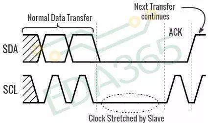
Clock Stretching is an optional configuration for the slave. If it is not enabled, the slave cannot control SCL; if it is enabled, the slave can reduce the transmission speed by forcibly pulling SCL low. During the period when SCL is VOL, the host can only wait for the Slave releases SCL.
Repeat Start
Sometimes the master needs to perform multiple message exchanges in one communication such as transferring messages with different slaves, or switching read and write operations, and does not want to be interfered with by other master during this period, then you can use the ‘repeat start condition’ —In a communication, the master can generate multiple start conditions to complete multiple message exchanges, and finally generate a stop condition to end the entire communication process. Since there is no stop condition during the period, the master keeps occupying the bug, and the other mains cannot switch in.
Here’s the difference between UART, I2c, and SPI
| Protocol | Complexity | Speed | # of Devices | # of Wries | Duplex | No. of master and slave | |
| UART | Simple | Slowest | Up to 2 devices | 1 | Full Duplex | Single to Single | |
| I2C | Easy to chain multiple devices | Faster than UART | Up to 127, but gets complex | 2 | Half Duplex | Multiple slaves and master | |
| SPI | Complex as device increases | Fastest | Many, but gets complex | 4 | Full Duplex | 1 master, multiple slaves |
You might be wondering, which of these three communications is the best? Is it UART, I2C, or SPI?
Unfortunately, there is no “best” communication peripheral. Each communication peripheral has its own advantages and disadvantages.
Therefore, users should choose the communication peripherals that best suit their project. For example, if you want the fastest communication peripherals, SPI would be ideal. On the other hand, if the user wants to connect multiple devices without being too complicated, I2C would be ideal as it can connect up to 127 devices and is easy to manage.
Here are Some Product that supports I2C Communication Protocols
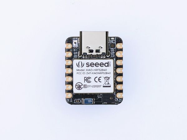
All the XIAO Series Microcontrollers that support I2C, UART, or SPI, and here’s the link for you to take a look at it Seeed Studio XIAO Series. And now for most of the XIAO Series is Free Shipping!
Here are some features of the XIAO Series
- Thumb-sized form factor, only 20×17.5mm. Made for space-constrained scenarios.
- Up to 11 available IOs support multiple interfaces, including analog, digital, IIC, UART, SPI, and more.
- Powerful core with a strong performance for diverse and complex applications.
- Single-sided components, surface mounting design. Easily integrate XIAO into other boards for mass production.
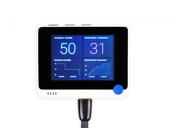
Wio Terminal is an ATSAMD51-based microcontroller with both Bluetooth and Wi-Fi Wireless connectivity powered by Realtek RTL8720DN, compatible with Arduino and MicroPython.
Here are some feature of the Wio Terminal
- Powerful MCU: Microchip ATSAMD51P19 with ARM Cortex-M4F core running at 120MHz
- Reliable Wireless Connectivity: Equipped with Realtek RTL8720DN, dual-band 2.4Ghz / 5Ghz Wi-Fi
- Complete system equipped with Screen + Development Board + Input/Output Interface + Enclosure
- Raspberry Pi 40-pin Compatible GPIO enables installation as a peripheral to the Raspberry Pi
- Support Arduino, CircuitPython, Micropython, ArduPy(What is ArduPy?), AT Firmware, Visual Studio Code
- USB OTG Support
I purchased a Seeed Grove kit and I want to control a 4 channel Seeed relay board using I2C. Is there an example of using the I2C bus to control this relay. I can trace the python code down to compiled python modules but without a map of the overall software construction, I’m lost as to how to proceed. Thank you.
Maybe this link might be able to help you solve that problem, If not you can ask our Technical support team about that at : techsupport@seeed.io
Here’s the link:
https://www.seeedstudio.com/I2C-CAN-Bus-Module-p-5054.html?queryID=16e32b893f10a0adbba9195798bb90b1&objectID=5054&indexName=bazaar_retailer_products