Seeed Fusion Updates V0: PCBs and the Pandemic – Understanding Manufacturing and Cost
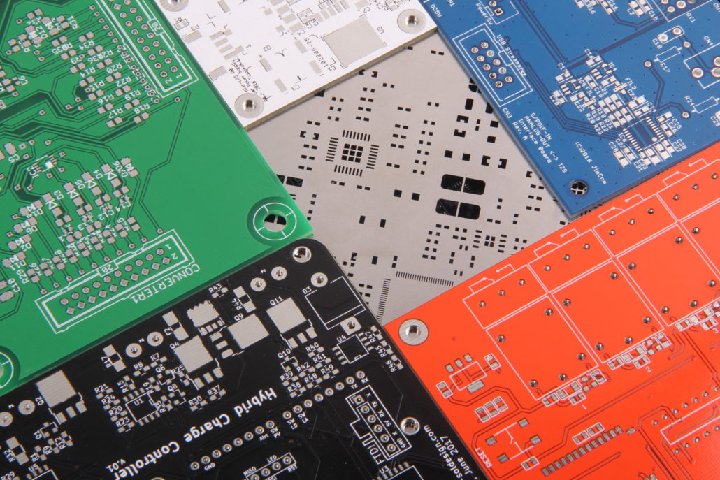
As widely reported, one of the consequences of the pandemic has been a worldwide chip shortage. But chips are not the only materials that have become more costly. Global restructuring and measures taken by financial institutions in the west have had far-reaching and long-lasting consequences across all manufacturing fields and their supply chains. In terms of manufacture of bare PCB boards, the primary expense pertains to the substrates and surface finish materials such as ENIG. But instead of implementing a blanket price hike on all boards, we and others in the industry have chosen to target boards with specific combinations of features that are less common.
In the following weeks and months, we will be updating Seeed Fusion webpages in stages, including the addition of tools and smarter implementations to ultimately make the experience more convenient and faster. Expect a new Gerber Viewer, CAD downloads for the OPL and more.
In the first phase launching next week, there will be some spring cleaning with certain combinations of parameters being removed. And in this article, we thought it would be interesting to talk about some of the challenges faced by manufacturers on the lower end of the cost spectrum and the factors that influence their decision-making.
In a short, the Seeed Fusion quickturn service is able to offer cheaper prices compared to traditional fab houses is largely due to volume. With enough volume, similar orders can be pooled together and production facilities can be streamlined. For example, the default 1.6mm thick boards with green solder mask and HASL surface finish are the most common, meaning there is plenty of boards to fill the production panels fully and use the same tools and materials again and again, minimizing waste and maximizing efficiency.
Rarer combinations however, increase the chance of empty space on panels and wasted materials. The fewer orders available to pick from, the harder it is to find boards to fit in the empty spaces. For example, 1.2mm thick boards with red solder mask: a production panel can only be one thickness and typically only have one color. The same goes for copper thickness. The whole panel must be dipped into the plating solution to make up the higher copper thickness.
Different lead times may also affect which boards can be panelized together. Features that require additional production steps, such as plated half holes/castellated holes, would extend the lead time of all the boards on the panel. In the current climate of fast, quickturn PCBs, sometimes that delay is just not acceptable.
There are two main ways of reducing panels for uncommon boards:
1. Charge more for such boards and
2. Don’t accept them.
Those that fall in the latter category are typically on the extreme side. Feedback from customers tell us which features are more important than others, which plays a part in determining if a combination is restricted or axed. Others may be restricted due to increased production difficulty or a higher risk of defects. Here are some of the changes made in the Seeed Fusion update V0:
2oz Copper Weight
2oz copper weight is now restricted to 1.6mm or 2.0mm board thickness and cannot be selected with Red, Yellow or Matte Black solder mask. 2oz copper weight cannot be combined with impedance control.
Higher copper weights are relatively uncommon. There are other techniques available to designers to increase current carrying capacity and when given the choice between color, copper weight or board thickness, most of our customers chose to forfeit the heavier copper.
Castellated holes/Half plated through holes:
Boards with castellated holes can now only be 1.0mm or 1.6mm thick.
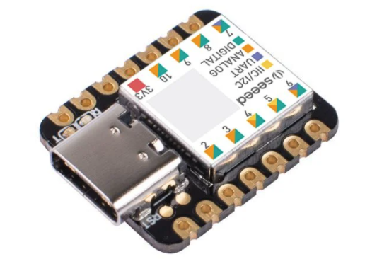
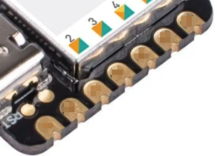
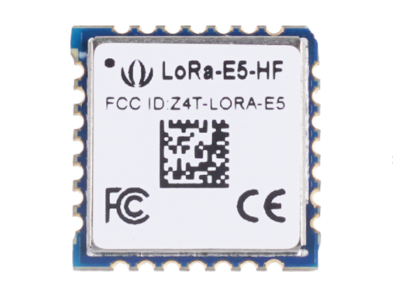
Boards with castellated holes tend to be modules like Wi-Fi modules and the Seeeduino XIAO. They tend to be small and have plated half holes on multiple sides, even all sides like the LoRa-E5, which limits the space available for tabs to hold the boards to the rest of the panel. If the boards are too thin, they could easily break from the panel mid-production, jeopardizing further processing. Thicker boards contribute to stronger panels during production.
0.6mm Board Thickness
0.6mm thick boards cannot be combined with HASL or Lead-Free HASL. Black solder mask is also not available.
The thinner boards are more likely to snap off from a panel during handling, routing or drilling. 0.6mm boards are so fragile, that they could warp or break during the HASL surface finish process, which physically applies force against the boards.
Single Layer Boards
Few people prefer single-sided boards given the choice of double-sided boards at the same price yet there is still a demand for them. Most single layer boards are very basic and some options have been restricted to reflect this and the lack of plated holes
Other Changes:
Aluminum boards: Aluminum board options have been tidied up and the default options have been changed to that of Aluminum boards with special pricing. Uncommon thicknesses have been removed and the prices modified.
Advanced and Premium PCB services: These services do not pool orders together. Each consignment is treated individually and production is tailored to the specific design, so the same restriction tactics cannot be applied. For that reason, the price increase directly reflects the increase in substrate materials.
That is all for now in V0. Look out for the coming updates where we make the charges for restricted parameters visible on the order page itself and the Open Parts Library gets a new feature. As always. thank you all for your support and understanding and we’ll see you next time.