7 Most Popular PCB Testing Methods During Manufacturing and Assembly
In recent years, whether it’s manufacturers, hobbyists or emerging companies, the application of PCBA functional testing has gained widespread attention, perhaps this is due to the increasing emphasis on quality assurance, changes towards smaller batch manufacturing and subsequently the search for efficient testing methods.
The entire manufacturing process is complicated and is affected by a variety of factors. There may be hundreds of components and thousands of solder connections on a single board, and without adequate verification, the entire process is a hit and miss affair. Therefore, the electronics manufacturing industry and product developers meet this challenge by establishing various inspection and testing procedures to ensure the quality of their products.
Testing can help identify critical errors early on, increase yield and reduce costs, and improve overall quality and safety. PCB functional testing is one of the best and most versatile tools for verifying a board for usage in the real world, but it is just one of many testing methods in a manufacturer’s arsenal. With each testing method having its advantages and disadvantages, it can be difficult to determine the best test method for your situation and budget. In this article, we will review 7 of the most common PCBA testing methods.
1.Visual Inspection
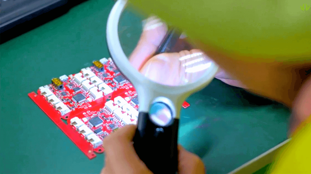
PCBA inspection can be generally divided into electrical and visual inspection methods. Visual inspection uses a magnifier or the technician’s bare eyes to manually find solder defects and other visible defects such as component orientation, missing components and board stains. This is the simplest and most basic inspection method.
Advantages:
- Cheap and easy to set-up – no test fixture or lengthy set-up required
- Most major solder defects can be identified
Disadvantages:
- Subject to human error. It May depend on the technician’s skill
- Time-consuming, labor-intensive and inconsistent
- Can only inspect visible solder joints – hidden joints and underside joints cannot be evaluated.
Applications: Ideal for simple designs with larger components and lower quantities.
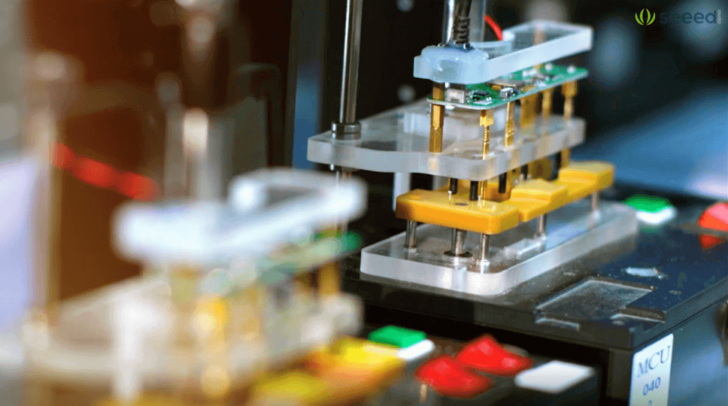
2. IN-CIRCUIT TESTING (ICT)
PCBA ICT is currently the most robust and popular type of PCBA testing for larger batches and mature products. A form of automated testing, the typical fault coverage is upwards of 90%. During PCBA ICT, electrical probes in a bed of nails format send currents through specific locations on the board at designated test points. These tests can check for shorts and open circuits, possibly due to missing parts, solder defects or incorrect orientation of diode/transistors.
For large or repeat batches, tailor-made test jigs can be made to perform in-circuit quicker and more efficiently.
Advantages:
- Fault coverage can be as high as 98%
- Efficient and quick method of testing mass-produced products
Disadvantages:
- Test jig is an additional expense.
- Not suitable for small batch production or prototyping as any changes to the design requires the test jig to be modified/re-made.
- Can only access test points, designer needs to add test points to the board.
- Cannot assess certain defects, e.g. excess or insufficient solder, voids.
Applications: Suited for testing mature products at high-volume.
3. FLYING PROBE TESTING(FPT)
A form of in-circuit testing, flying probe or flying needle testing is often seen as an improvement over bed-of-nails ICT. As well as test points, a flying probe machine can also access untented vias or the ends of components themselves to be used as test points, and can be programmed to check the value of passive parts, directly check diode/transistor orientation and perform voltage measurements. There is no need for a tailor-made fixture, and any changes to the components or PCB design only require updating the software.
Advantages:
- Cheaper and faster to implement or modify. No fixture required.
- Higher test coverage – able to use vias and component pads as test points.
- No need to add test points. Save board space.
Disadvantages:
- Testing is too slow for mass testing
- Cannot assess certain defects, e.g. excess or insufficient solder, voids.
Application: Prototypes, small and medium batch production or small boards with high component density.
4. AUTOMATED OPTICAL INSPECTION (AOI)
AOI uses a single (2D) or two (3D) cameras to take high-resolution images of the PCB, and then compares these with images of a template board of the design being tested, or with a database of images of good and bad boards. An AOI machine can be added to the end of the production line directly, serving as the first line of quality assurance and allowing for adjustments to be made to the production process in-situ.
AOI covers all the checks manual visual inspection would identify with greater accuracy and consistency and can identify incorrectly placed components if visibly distinguishable.
The template method is more accurate, however this is time-consuming to set-up and is not suitable for prototype designs subject to changes.
Advantages:
- Most major solder defects can be identified.
- More consistent and accurate than manual visual inspection.
- Can be added to the production line directly for early detection of defects.
Disadvantages:
- AOI is a passive testing method – can only detect surface defects. Difficult to provide 100% coverage.
- Set-up and programming for template matching is time-consuming and must be re-done with every design change.
- Database-based matching may not be as accurate and depends on the quality of the database.
Application: Suited for testing mature products at high-volume.
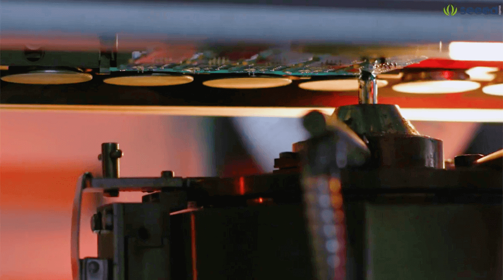
5. AUTOMATED X-RAY INSPECTION(AXI)
Compared with other inspection methods, AXI testing technology is unique in that x-rays are used. X-rays can penetrate the PCB and body of components to generate 2D or even 3D images of the solder joints. This makes it ideal for hidden joints such as those on Ball Grid Arrays (BGA) and other underside pads. AXI inspection can also detect solder voids and many other optical inspection methods cannot.
When used alongside the production process, AXI can be a useful tool for detecting defects early on, thus allowing engineers to make process adjustments to eliminate the source of the issue. This reduces the number of boards requiring costly repairs. For small batches or prototyping, x-ray inspection of only the chip components with hidden pads is often sufficient.
Advantages:
- Can have the highest defect detection rates of common inspection methods.
- Emphasis on long-time solder joint quality, not just connections.
Disadvantages:
- Well-trained and experienced operators are required.
- Very time-consuming and expensive process
Application: Volume production and complex boards with chip components.
6. BURN-IN TESTING
The burn-in testing is very effective and accurate, allowing you to check the performance and find hidden defects before the boards go out into the field. During burn-in testing, boards are subjected to conditions exceeding the rated operating conditions to detect early failures and test load capacity, thereby eliminating premature failures in the field. Unlike many inspection methods, that only check for indicators for potential failure, burn-in testing simulates extreme operating conditions to trigger failures.
The operating conditions tested can include temperature, voltage/current, operating frequency or any other operating conditions relevant to the design. The data collected through this process can in turn help engineers understand the cause of the defects and optimize the design or manufacturing process.
Advantages:
- Checks performance in real environmental conditions that other testing methods cannot.
- Greater product reliability
Disadvantages:
- The testing process may shorten the product’s lifespan
- Reduces overall yield
- Time-consuming and labor-intensive process
Applications: Equipment that may operate in extreme environments or where failure is not acceptable, e.g. medical or military equipment.
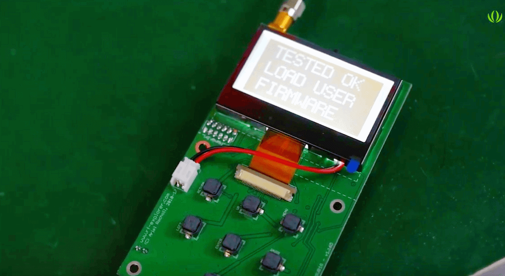
7. FUNCTIONAL TESTING (FCT)
Functional testing is performed in the last phase of production to serve as the final quality control procedure. In short, it ensures that the device under test (DUT) operates as intended. Depending on the complexity of the design and the specific testing requirements, functional testing can be as simple as an on-off power test, to a comprehensive test with strict protocols and testing software.
Because of this flexibility, functional testing can be employed as a substitute for more costly testing procedures. Functional testing simulates the actual operating environment and therefore can be more direct than other testing methods. However, it may be more difficult to ascertain the cause of any defects and unlike burn-in testing, functional testing will not catch boards that fail early in the product’s lifecycle.
Complete 100% functional testing is increasingly being used with small-batch manufacturing to ensure every board coming off the production line is operational.
Advantages:
- Flexible and highly customizable. Almost all types of PCB can be tested.
- Cheaper and more convenient than other testing methods that require specialized equipment.
Disadvantages:
- Defect detection rate depends on the checks covered by the test plan.
- Trained technicians required to isolate the cause of the defect.
- Under stress, the board may still fail shortly after passing functional testing.
Applications: Ideal for small-batch manufacturing, or in conjunction with other testing methods.
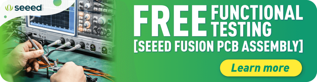
Attention! For the first time ever, we’re bringing you Free Functional Testing for ALL PCBA Orders! Seeed Fusion functional testing ensures the quality of PCBA products and avoids delays in product release due to rework. Come and get the first try!
Seeed have been focusing on electronics manufacturing and assembly for more than 10 years with circuit board test qualifications and complete test items. Seeed Fusion provides functional testing (FCT) and other testing and programming services for PCB assembly orders. We test your products according to your needs and applications, helping you to quickly verify the products accurately at reasonable prices. Get a quote now!