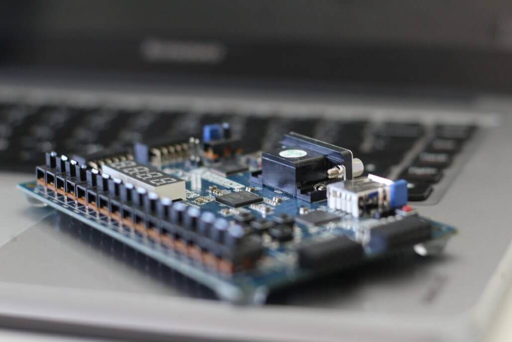
What is an FPGA and why use them?
An FPGA (or Field Programmable Gate Array) is an integrated circuit that can be reprogrammed after manufacturing. As the name aptly suggests, FPGAs are made up of arrays of logic gates (AND, OR, XOR, etc.) that can be configured in the field (more about this later). In contrast, hardwired circuits are designed to serve specific functions that cannot be changed after production.
In our previous article, we provided a detailed introduction to FPGAs and FPGA Dev Boards, their uses and benefits. Read more about FPGAs in our FPGA and FPGA Dev Boards – What is it and What are they used for? introduction.
Today, we will focus more on the principles behind FPGAs and what makes them relevant to the electronics world.
FPGA Architecture
An FPGA consists of a number of configurable logic blocks and I/O blocks, as well as programmable interconnects. In addition, they will carry clock circuitry for driving clock signals to each logic block.
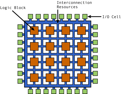
Configurable Logic Blocks (CLBs)
The logic in FPGAs is stored in configurable logic blocks (or CLBs).
We can think of CLBs as the individual building blocks that make up the FPGA. These building blocks are each programmed to perform a specific function both effectively and efficiently. It is the flexibility to program and connect a variety of CLBs that gives FPGAs the versatility that they are known for!
A CLB contains several smaller components, including:
- RAM for creating lookup tables (LUTs) for combinatorial logic
- Flip-flops or registers for storage
- Multiplexers for routing logic internally and externally
In modern FPGAs, each CLB contains sufficient logic to create a simple state machine.
Configurable I/O Blocks
Configurable I/O blocks handle the input-output signals going into and out of the FPGA.
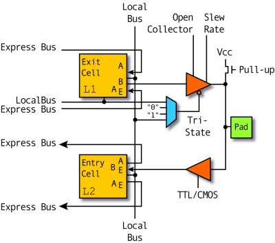
These I/O blocks typically have an input and output buffer with three-state and open collector output controls. Pull-up resistors are typically used on the outputs, while pull-down resistors may be utilised for terminating signals or buses without external discrete resistors.
In addition, there a number of things that we can configure at the output:
- Output polarity can be programmed for active high or active low output
- Slew rate can be programmed for fast or slow rise and fall times
- Flip-flops on outputs for low-latency, direct output of clocked signals to pins
Programmable Interconnects
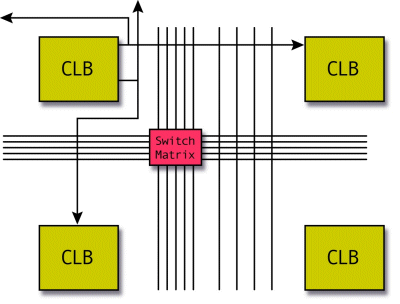
Interconnects are used to connect CLBs to each other, and consist of long lines for connecting far apart CLBs. For connecting CLBs that are near to each other, short lines are used instead. These lines are controlled by switch matrices in the FPGA, which will enable / disable these connections as per the desired combination.
Clock Circuitry
The clock circuitry of an FPGA are made up of special I/O blocks with high drive clock buffers known as clock drivers. They drive clock signals onto the global clock lines.
Global clock lines are specially designed long lines that are made up of three-state buffers. They are specially designed for low impedance and low-latency propagation.
As you might guess, these lines are connected to clock buffers and the clocked elements in the CLBs. This is how the processing timings are matched up throughout the FPGA, minimising the differences caused by clock signals arriving at different timings in different parts of the chip.
Microcontroller or FPGA?
The typical computers and microcontroller that we interact with every day carry what we call ASICs (Application Specific Integrated Circuits).
“Application Specific” means that they are designed for a single function for their entire operating life. The digital circuitry and thus the internal logic of ASICs are permanently drawn into the silicon of the chip. Because of this , software for ASICs have to be built around the chips instruction set.
An Example: Button-triggered LED
Let’s say we want to turn on an LED when a button is pressed.
On a microcontroller like Arduino, we write some code in Arduino or MicroPython that the Arduino hardware understands, so that it uses existing circuits to perform the function. The hardware is instructed to check for the input continuously at the button’s input pin, then to update the LED status accordingly.
If we programmed the same function on an FPGA, there would be no need to check the input pin status as the button and LED would be directly connected as a digital circuit of its own! Compared to the Arduino microcontroller, this cuts out the need for the processing power used with all the additional instructions required.
FPGA’s Advantage: Efficient & Scalable
Although the power savings and speed gains aren’t significant in the simple example we’ve just shared, you can imagine that these can become critical when our processes are far more complex.
Furthermore, because FPGAs are made up of modular CLBs and configurable interconnects, we can form multiple such circuits in a single FPGA. This is what is meant when FPGAs are described as inherently parallel.
Starting with FPGA
Now that you understand and have set your mind on FPGAs, you might be wondering how to get started.
We will first go through a demonstration adapted from FPGA4Student, which shows how a full adder circuit can be programmed onto an FPGA.
To begin our circuit design, we first obtain a circuit schematic like below. Note the use of XOR, AND, and OR digital logic gates in the circuit design.
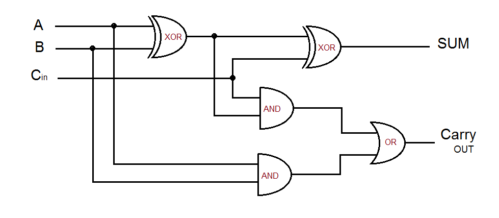
To program our circuit onto the board, similar to software programming, we will have to use a HDL or Hardware Description Language to define our desired circuit. Two popular options are Verilog or VHDL.
Code in Verilog
module full_adder(input A,B,Ci, output S,Co);
  wire tmp1,tmp2,tmp3;
  xor u1(tmp1,A,B);
  and u2(tmp2,A,B);
  and u3(tmp3,tmp1,Ci);
  or u4(Co,tmp2,tmp3);
  xor u5(S,tmp1,Ci);
  endmodule
We can see that the code simply defines the circuit according to the schematic design – which can then be uploaded to our FPGA board.
Take note that with greater complexity, rigorous simulation and testing of our FPGA designs will become necessary before uploading. Nonetheless, we have seen how a simple circuit can be defined with a HDL.
FPGA Development Environment
There are many available platforms to begin FPGA programming. However, FPGA programming and prototyping is still a complex process – meaning that many development softwares can come with complicated interfaces and tools that may overwhelm a beginner.
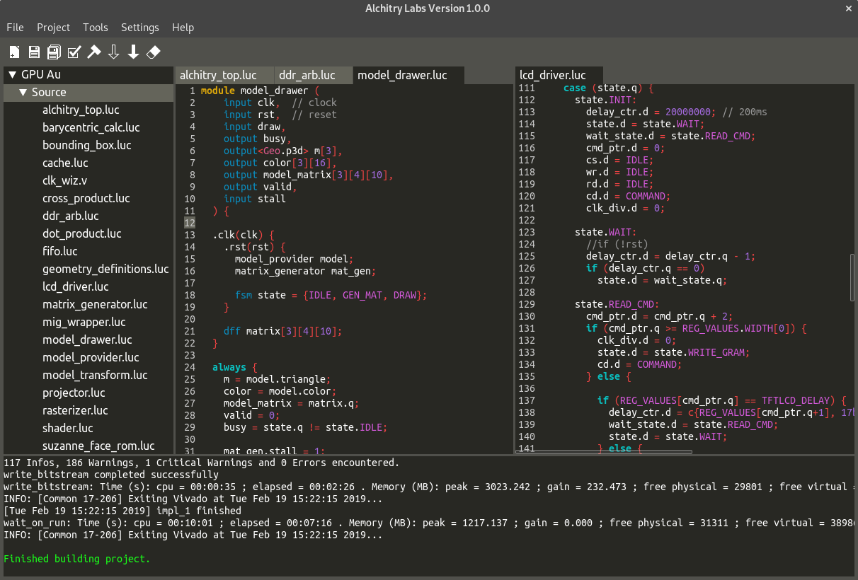
If you are new to FPGAs, you should definitely try Alchitry Labs, which offers a beginner-friendly experience. It also offers support for Lucid, a simplified and easier to use HDL based on Verilog.
Pick Up your own FPGA Board!
If you are ready to dive into the great possibilities offered by FPGAs, we recommend the following boards to get started.
Most Affordable Board: Sipeed Tang Nano FPGA Board Powered by GW1N-1 FPGA
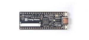
The Sipeed Tang Nano FPGA board is a very good option for curious beginners. At a low price of under $5, the board features rich I/O options and will allow you to familiarise yourself with FPGA programming before deciding your next step.
However, take note that due to the small size of the board, complex calculations such as accumulation or multiplier cascading will not be possible.
Python-Compatible Board: PYNQ™ Z2 board – based on Xilinx Zynq C7Z020 SoC
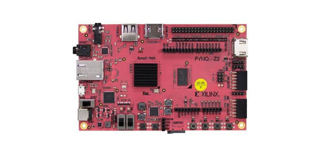
The PYNQ™ Z2 board is a good option if you want to explore FPGAs without explicitly learning a HDL. The board is supported by PYNQ, which is an open-source project from Xilinx that enables programmable logic to be done via the Python programming language and its libraries.
Best General Purpose FPGA Board: Spartan Edge Accelerator Board – Arduino FPGA Shield with ESP32
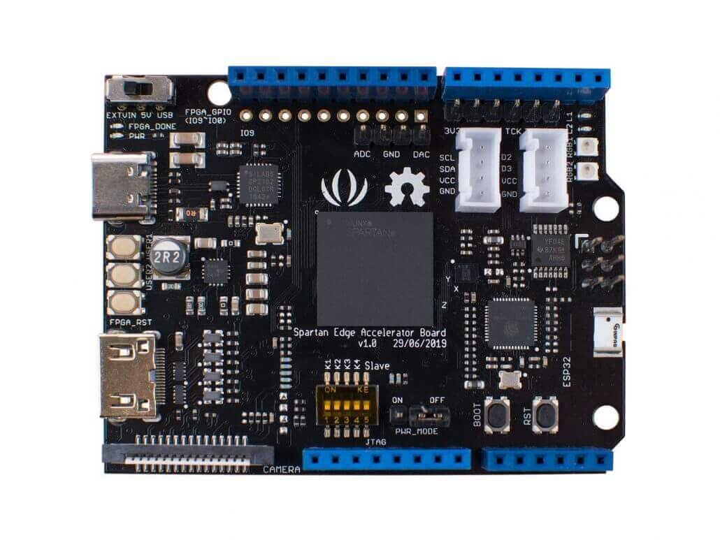
The Spartan Edge Accelerator Board combines the advantages of Arduino and FPGA to deliver a comprehensive experience to developers. The board is supported by a full Arduino FPGA API, which enables control of FPGA I/Os with the beginner-friendly Arduino IDE.
Useful Learning Materials
Since FPGAs are very versatile, there is a lot of knowledge and technique to be learnt. To understand more about the fundamentals of circuit design, we recommend the Introduction to Digital Circuits Series by Renesas.
Otherwise, you might be interested in the following FPGA online courses:
- Learn the Fundamentals of VHDL and FPGA Development – Udemy
- Intel’s Online FPGA Training Curricula
- Learning FPGA & Verilog for Beginners – Numato
- Introduction to FPGA Design for Embedded Systems
Many universities also now offer formal introductory and advanced classes on FPGA design for their electrical engineering or computer engineering majors.
Reconfigurable hardware with FPGAs are becoming even more popular over time. For our dear readers who are still in or have not yet attended university, we strongly encourage you to include FPGA knowledge and design classes in your study plan!
Summary
We hope that you have learnt more about FPGAs in today’s article. Although FPGAs may seem daunting, FPGAs are becoming increasingly popular and the learning will surely be worth it in the end!
Not sure what you would do with an FPGA board? Check out Xilinx SEA-7 FPGA Projects Collections – from Xilinx Summer School for some interesting ideas!