PCB Coil Board Design for Manufacture

Requests for PCB coil boards are becoming more and more common and demanding. However, the nature of these designs present a unique challenge to PCB fabricators. In this article, we present Seeed Fusion’s experience dealing with this kind of situation and provide suggestions when using our PCB manufacturing services.
Coil circuit boards, sometimes referred to as RF coil or spiral coil boards, refer to a design where a single trace coils around itself in a spiral-like pattern. These designs have gained popularity as onboard planar inductors, instead of using a physical inductor component to save space and money. In the past, the technique was used extensively for IR receivers but notably gained popularity when a designer used multiple coils in a multi-layer PCB to create a miniature PCB motor. However, few truly understand the difficulty in producing such boards.
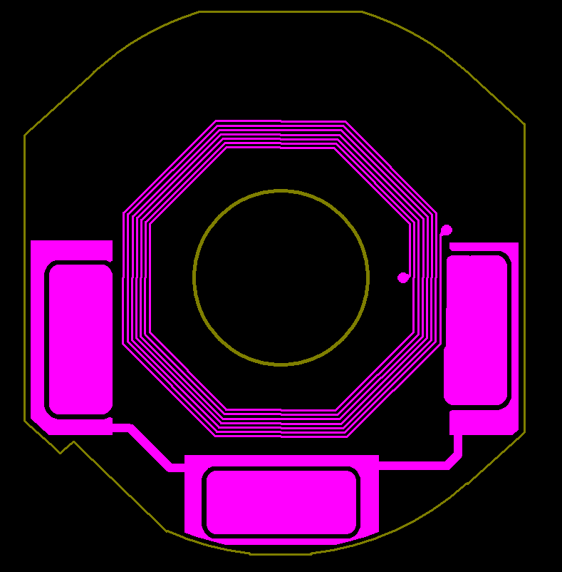
With capable quickturn services popping up here and there, it is easy to take for granted how the ‘cheap’ PCB industry has advanced over the years. Improved manufacturing capabilities across the PCB industry have seen 4 mil (0.1 mm) trace widths and spacings become more and more common. But coil designs are an exception and some of the most effective quality control techniques are inept at guaranteeing the electrical integrity of such designs.
Not too often we find ourselves in the situation where a customer has an inductor coil design but the trace width and spacing is insufficient. The customer then (sometimes angrily) points out that they had selected the correct trace width/spacing option and therefore, there should not be any problems. While taken at face value, that is true; the situation is not as simple as that.
Trace Width and Spacing
Typically, fab houses will specify a minimum trace width and spacing parameter in the capability specs. The smaller this value, the greater the care and process control that needs to be implemented to ensure no shorts or breaks. For example, on the Seeed Fusion standard order page, we have options for different levels of difficulty from the standard 6/6mil (read as 6 mil trace width/6 mil trace spacing) down to 4/4mil with subsequently increasing costs. With improvements in technology and methods, smaller values are becoming more and more commonplace. With the Seeed Fusion Advanced PCB service, 3/3mil is possible.

Now, take a moment to think about how your PCB design software helps you detect circuit shorts or breaks during the layout phase or a design rule check. They use the netlist from your schematic to determine whether two points in the circuit layer are supposed to be connected. In the PCB factory, they create a netlist from the Gerber files and in-circuit-testing (ICT) methods such as flying needle or bed of nails tests use this to confirm the correct circuit continuity between two exposed contacts.

Flying Needle Testing 
Bed of Nail Testing
With smaller circuit widths and spacings, the danger of shorts caused by manufacturing processes becomes a real issue and that’s where ICT really comes into play. In conjunction with AOI, ICT methods serve as an insurance policy against shorts and breaks with a typical success rate in the high 99%.
However, an inductor coil design is different in that a single turn can be surrounded on both sides by turns of the same trace. This makes it virtually impossible for ICT to detect shorts between two turns. They are undetectable. According to the netlist, they are the same trace and so it’s ok if one round of the coil is merged with the next.
In addition, shorts are more likely to occur due to the sheer compactness of such designs. There isn’t much room to accommodate plating tolerances and so for those reasons, the ability to reliably achieve 4/4mil or even 5/5mil spacing is much more difficult. Without ICT, quality assurance technicians are reduced to relying on AOI or by meticulously inspecting the boards visually.
The issue is elevated for batch processing, where tolerances are much more difficult to control, so many manufacturers set different trace width/spacing limits for coil boards. At Seeed Fusion, with the standard quickturn service, we recommend at least 6/6mil spacing for the coils. Any lower may be achievable but involves additional wastage and labor costs. Note that not all fab houses are willing to undertake such requests. No one wants to inspect traces covered in black or white solder mask oil with their bare eyes.
If 6/6mil is not acceptable, the Seeed Fusion Advanced PCB service can handle true 4/4mil spacing. Just upload your design to submit a quotation request.
So, take these notes into consideration the next time you are counting the turns in your next RF design, and bear in mind the extra inductance for a given coil size may not be possible at your favorite quickturn service.
too much problems, bla-bla, but
“If 6/6mil is not acceptable, the Seeed Fusion Advanced PCB service can handle true 4/4mil spacing. Just upload your design to submit a quotation request.”
well, if you claim it is possible – just do it.
Different production methods, different price