Seeed Fusion Introduces New Detailed Production Status Updates for PCB and PCBA
It’s been on our to-do list for a long time and you’ve constantly been nagging at us to get it done – now it’s finally online! We’ve upgraded the PCB and PCB assembly order production statuses so you can have a better idea of how your order is coming along. Worried your order has gotten stuck? Taking a little longer than usual? Just log into your account, go to your Order History and click for more details.
*Please note that not all PCB orders (notably Premium and Advanced orders), will have detailed production statuses, but that does not mean they are not being processed! If in doubt, ask our support team.

PCB Production
Now for the interesting bit. We’ve broken down the PCB manufacture phase into 12-14 steps. To give you a better idea of what goes on at each stage, here’s a brief introduction:
Panel Preparation
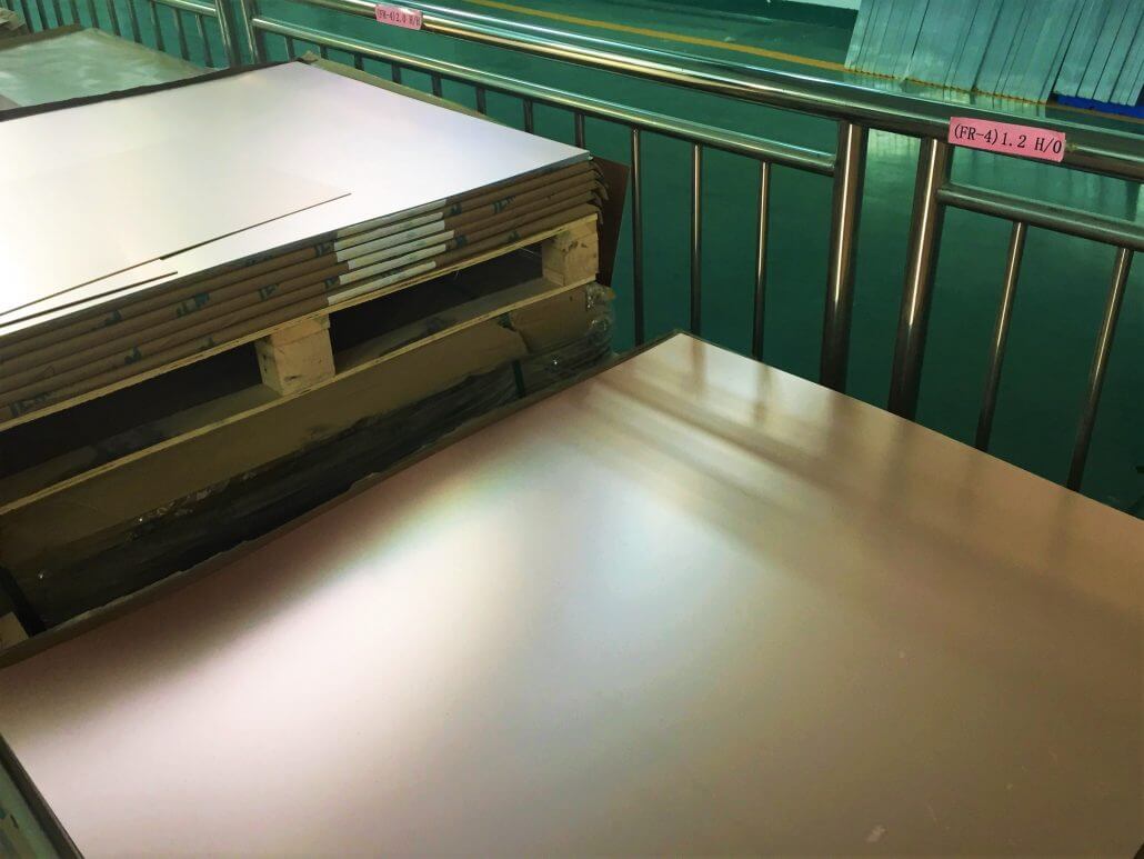
All boards begin as big sheets of FR4 fiberglass panels covered with copper foil on both sides (collectively known as a core). These get sliced up into manageable sizes – typically around about 40 by 50 cm panels and are then cleaned and pre-processed.

Inner Layer Etching
(4+ layer boards only)
For multi-layered boards, there are additional layers to process. The cores of the multi-layer board are etched first much in the same way as 2 layer boards to make the traces for the inner layers.
Inner Layer AOI
(4+ layer boards only)
All inner layers undergo Automated Optical Inspection (AOI) to visually check the bare circuits for defects. It’s important to fix these first as reworking the inner layers is impossible after the stack-up has been built.


Lamination
(4+ layer boards only)
Perhaps the most time-consuming step in the production of multi-layer boards. The stack-up is constructed by sandwiching the core or cores, foils and prepreg layers together with strong epoxy glue. Multiple boards are then loaded into a large lamination press and exerted to high temperatures and pressures for several hours to allow the epoxy to cure and harden.
Drilling
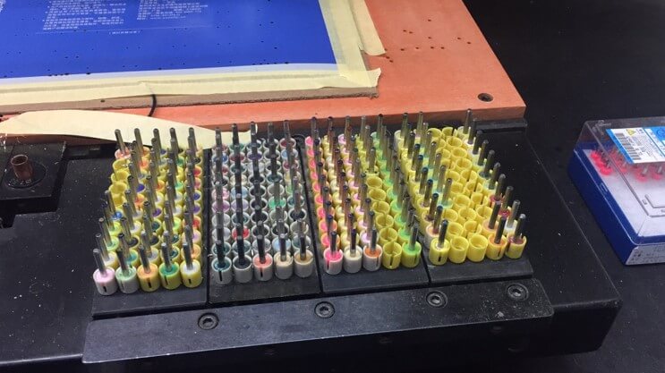
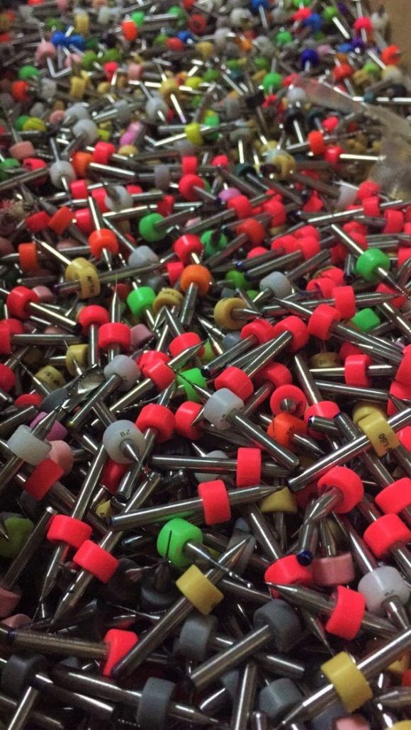
All the standard drill holes, including plated, non-plated holes and milling slots are drilled at this stage. The noisy thundering drill machines automatically change drill bits and sense if a bit needs replacing. At this stage, the freshly drilled holes do not have any copper plating.

Drill Hole Plating
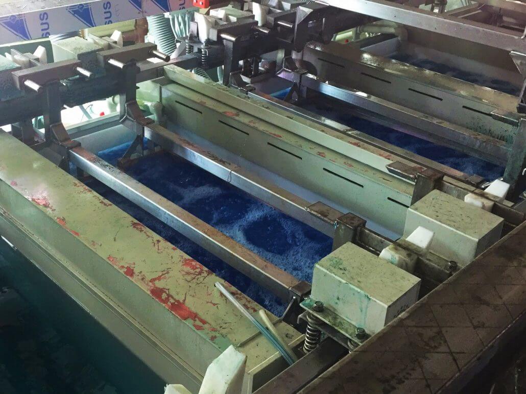
The first plating stage. The entire panel is hung on rails and dipped into copper sulfate baths to build the initial layer of copper on the walls of the holes. The thickness is only a fraction of the final copper thickness at this point.

Circuit Plating and Etching
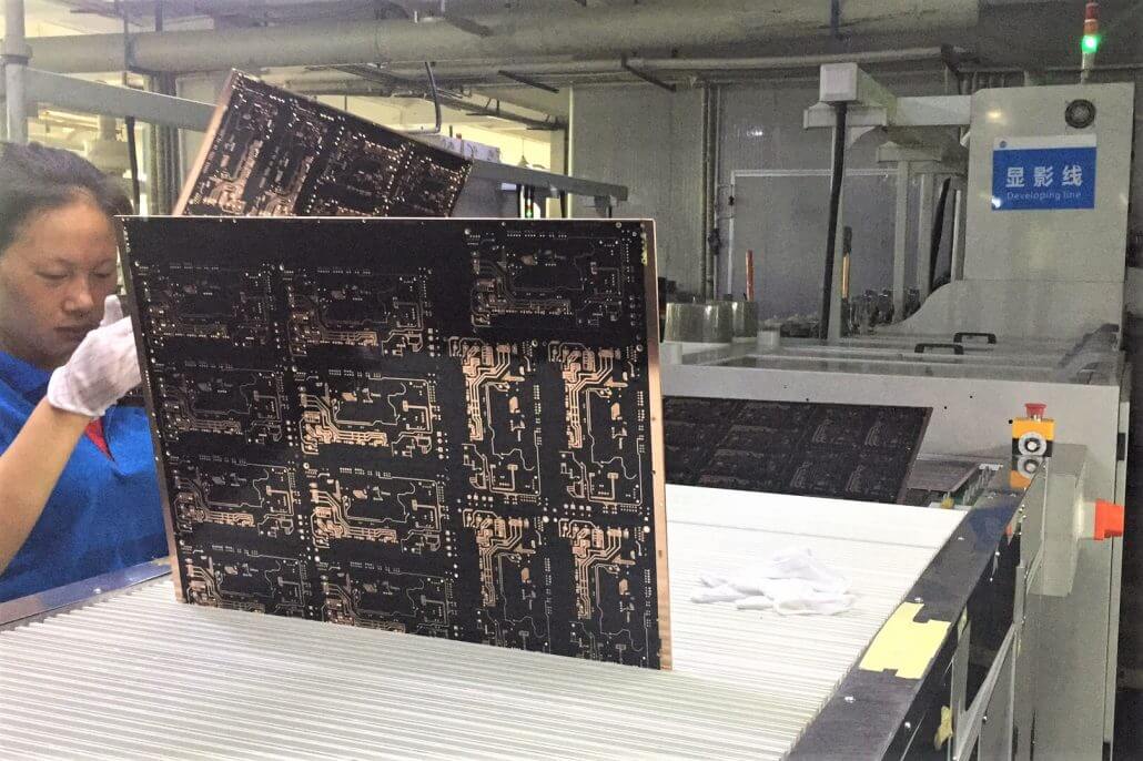
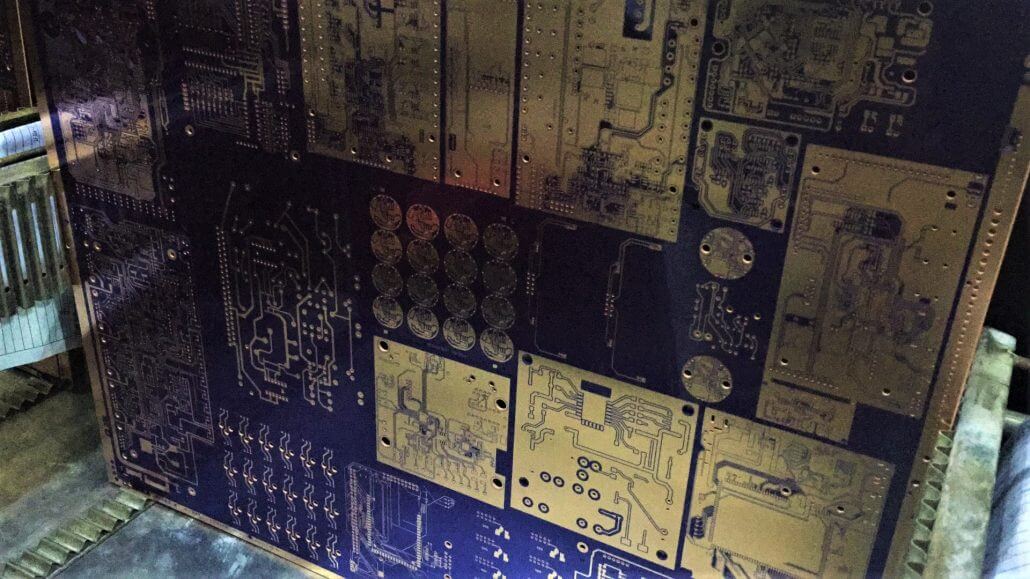
Several bathing, developing and etching steps are taken to build-up on the thickness of the copper features and remove or etch away the unwanted copper. Here the final desired copper thickness is achieved.

Outer Layer AOI
Automated Optical Inspection for the outer layers.
Solder Mask Application
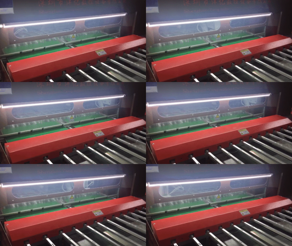
Solder mask (the main colored coating of the PCB) is applied using silkscreen equipment. The boards are then baked to cure the solder mask.

Silkscreening
The name is rather misleading now since white silkscreen text is now printed onto the boards using a specialized LaserJet ink printer. This only takes a few seconds and is more accurate compared to the traditional silkscreen method. (Black silkscreen ink is still applied using the traditional method).

Surface Finish Application
The boards are sent to have the chosen surface finish applied onto the exposed pads.

In-Circuit Testing
All electrical connections are checked via either flying needle tests (for small quantities) or fixture testing (batch production). They are compared directly against the production files, that’s why you won’t find any shorts or broken circuits on your boards unless they originated in the files.

Board Routing
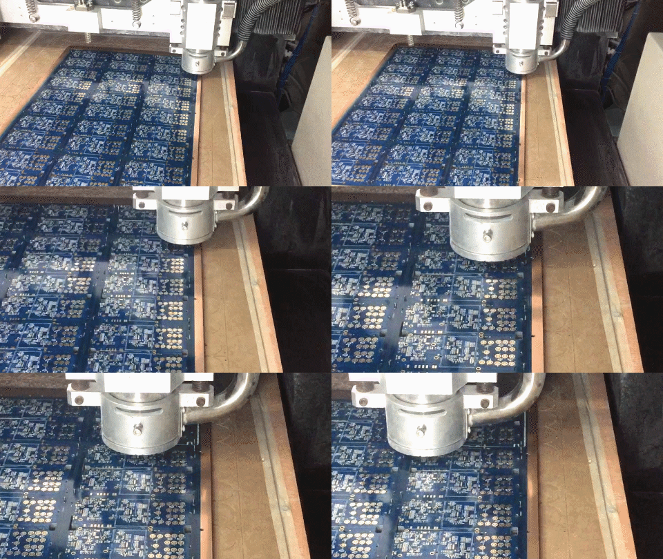
Time to free the boards from their panels. High-speed routing machines cleanly mill out the pieces, and boards requiring v-cuts are loaded into the v-cut machine. Boards with a lot of milling or many v-cuts can take longer to process.
Quality Checking
The boards are cleaned and meticulously inspected for
defects such as board warpage, blisters, solder mask ripple, exposed copper
edges, faded printing. After discarding defective pieces, the technicians count
if there are a sufficient number of acceptable pieces left. If not, then they
may need to produce another batch from scratch 


Think you know your stuff? Test your knowledge on the PCB production process!
Highlight the white spaces to reveal the answers
How many copper plating stages are there?
Two: one to give the plated through holes and vias a little copper covering and one to attain the desired final thickness.
If the copper layers in the core are 0.5oz thick (each side), and 1oz is the desired copper weight, roughly, what is the thickness of the copper walls of plated through holes?
>0.5oz, made up of the initial thinner plating and the final plating of the entire board. The actual value is greater and depends on the dimensions of the hole since a smaller area results in greater copper deposition.
In a standard production process for multi-layer boards, why is the copper weight in the inner layers thinner than the outer layers? What can be done to achieve the same or heavier copper weight for the inner layers?
Typically, there is no plating step for the inner layers so the final thickness is the same as the foil thickness of the core, normally 0.5oz. If more copper is needed, one could add another plating step and/or start with a core with a heavier copper foil.
How many sets (top and bottom) of photoimageable films have to be made for a typical 2 layer board?
Two or three, depending on whether or not the inkjet or silkscreen method is used for the silkscreen.
One set for copper etching, solder mask application and silkscreen,
At what stage are non-plated holes made?
At the drilling stage of course. All drill holes, whether plated or non-plated, are drilled together in one stage. The only difference after that is that all holes destined to be plated are exposed in the LPI film and non-plated holes remain covered up.
That’s all for now. Keep an eye out on your order statuses and stay tuned for next time when we’ll explain the PCBA production steps in more detail.