Demystifying ‘A’ in PCBA

Thanks to all who showed up for our first workshop on Saturday. It was a great success! As part of our Open Manufacturing effort, we want to share the knowledge with everyone.
To quickly walk through the birth of a hardware product. Most teams start with the design phase, including electronic design, structural design, or industrial design. This is the phase where you figure our whether the functionality you want to achieve can be done. In the prototyping stage, some people just use open source hardware modules, plug them together to achieve some functionalities. Then, once you figured out how things should work, we put them onto one customized PCB board, figure out the layout and produce a couple of quick prototypes to test it out, and then bom, you should have your product right?
We all wish thing are that simple. But most hardware entrepreneurs can probably testify that this is a long and grueling process, which requires a lot of manufacturing knowledge. This is why we are sharing this knowledge and here in the bay area to work with you all. Today we want to tell you how PCB assembly process works, and give you some tips and suggestions for making a good quality and functional board that achieve the functionalities you need in your product.

On a high level, it start with printing the solder paste on the board. And then do the surface mount which means putting the components on the board, which can be done with the pick&place machine. After you have placed all the SMD components on the board, we usually send the boards into the reflow oven to finish the soldering, this is what we call reflow soldering. The high temperature will melt the soldering paste and make sure the components stick on it firmly. And then we’ll go through the manual soldering stage for most of the boards because not all parts can be done by surface mounting, e.g. connecters with uneven surface, male&female headers. The last step is to clean off the dark marks that came from burning flux in the solder.
Printing Solder Paste

To print the solder paste on the board, you need to have a metal stencil with shapes that coincide with the pads on board. The metal stencil is usually laser cut with your PCB files, and the printing process can be done by the machine or manually.

This is what solder paste look like, it includes flux and metal powder of stannum, copper, silver. Nowadays we always use solder paste without lead in it but the boards would require higher temperature to melt. But this would put a higher requirement on the component selection as they would need to stand up to 250 celsius.
So that is why we say the design for manufacturing is really important. (Extended reading: PCB DFM Guide) As you selecting and sourcing parts, you need to incorporate all situations in the entire manufacturing process, so your components will not be damaged. Sometimes a simple part swop can save you a lot of time and money down the road. One of the ways we are helping makers is through our Open Parts Library — we like to call this parts with embedded supply chain solution.

Obviously we print solder on the board either by machine or by hand depending on the quantity. A whole assembly line usually compose of a print machine, a placement machine and a reflow soldering machine. A board just go through the machines from one to another automatically and finally become a nice PCBA. For quantity over a hundred, or a really complicated board, or if they have some BGA or very small 0201 components, we generally use the whole assembly line. For the prototype sample boards we usually do it manually to be quick and agile.
Surface Mount

Usually we’ll use machine when the quantity is above 50 or a hundred pcs. But sometimes it can also be used when we got some small quantity but complicate board or with large amount of components on each board.
Pick and place machine have large and small kinds too. In Shenzhen, we use some very big ones to place components that require a higher level of precision. The desktop version are limited to placing 0402 components. But for prototyping stage in small quantity, the functionality would be sufficient. The process starts with taking the PCB file and use software such as Altium Designer to export the coordinates of the components. Then edit them into a format that the machine can read. Unfortunately different machines have different format they adapt and it’s a bit of a process to convert the files. But with some experience, this can usually be done in an hour of so.
Sometimes the board is really kind of simple or we don’t have the PCB file right now, so we have to edit on the machine directly. And it can also be very quickly. Even you have finished the program on your computer, you still need to check out if all the positions where your coordinate located is absolutely correct. So the operating directly on the machine is very important.
The working principle of a pick and place machine is not very complicated. It takes components that are fixed on strips in different stacks, so that you can choose different kinds of components by editing the stack number in your program. Recently, we have been hosting workshops to give people some hands on experience with the pick and place machine. Join our meetup group to learn more.
Reflow Soldering

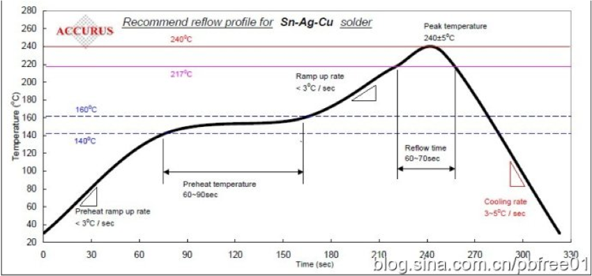
The reflow oven takes the board through different stages of temperature that controls the solder to melt and solid. The chart below shows the temperature curve. The entire process takes about 5–6 minutes.
Manual Soldering
If you are a maker yourself, chances are that you have hand soldered at some point. This is a really important process, and even for the large-scale manufacturers like Foxconn need to do lots of manual soldering works. Not all components can be placed by the place machine, the connecters, headers, et cetera. In other chases, some components can’t stand the high temperature during the reflow process. The other important reason is that sometimes the board is not soldered perfectly, or it has broken, so you have to repair it manually. So no matter how much pieces you made and what process you go though, you almost always have to do the manual soldering.
Cleaning

So last step is cleaning the board, mostly just to make the board look clean and nice. Since we usually use flux in manual soldering, high temperature will make the board to darken or leave black marks after heating by the solder iron. This process can also done by an ultrasonic cleaning machine or manually, and we must use a kind of liquid cleaner. Washing by machine is really fast and clean, but sometimes we also got some components cannot touch the liquid cleaner or maybe damaged by ultrasonic, for those, you will have to do it manually.
So now you probably understand why selecting a good, quality and solid BOM list is really important. Besides achieving the functionality you want to achieve, the parts you select will also affect your manufacturing process and hence cost as well. Weighing what you absolutely need and what are the tradeoffs is fundamentally important. But you may not have all the available information you need to make all the decisions upfront. This is why you need a DFM review, ideally from people who are able to think about hardware product design from the perspective of manufacturing (hint: Why SeeedStudio Fusion PCB Assembly).
Content credit: Danny Chen